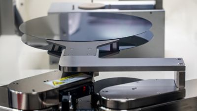
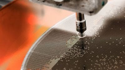
晶圆片及后道制成工艺的半导体检测

  • 质量控制:确保晶圆生产过程达到高质量标准
  • 尽早识别和调整晶圆工艺偏差,以提高产量并减少停机时间
  • 确保长期可靠性,消除可能影响设备性能的潜在缺陷
semiconductor

选择半导体生产中需要检测的领域

Wafer Production

Our advanced inspection solutions detect defects on surfaces, edges, and inside the wafers. We offer defect classification, metrology, and data management to support manufacturers in maintaining quality throughout the wafering process.

iStock 1174954855

Back End Process

With our advanced 2D and 3D inspection systems, we ensure comprehensive quality assurance by inspecting chips individually from wafer to packaging. This guarantees that only flawless components reach the customer and improves traceability and ROI.

back end process

晶圆片生产

ISRA VISION的半导体制造检测工具包括晶圆表面、边缘和内部的缺陷检测。缺陷分类、计量和数据管理是我们解决方案的补充,有助于制造商在整个晶圆片制造过程中管理质量。

了解更多关于我们的晶圆生产解决方案.

联系我们的专家

伊斯拉视像设备制造(上海)有限公司

董长生

半导体项目经理
上海
China

电话: +86 183 170 101 82 

电子邮件: info.china@isravision.com

Tony Dong